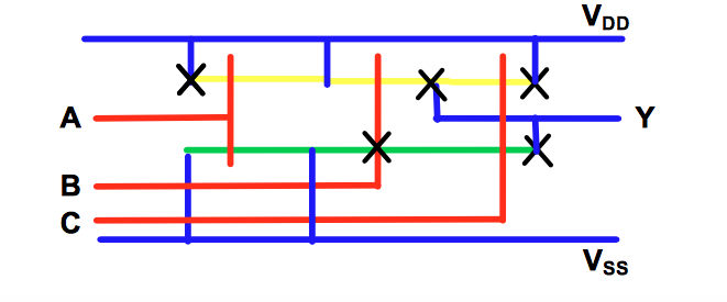
sketch a stick diagram for a cmos 4-input nor gate
Solved vss figure 2 5 circuit for cmos 3 input nor gate chegg com chapter 9 problem 10e solution vlsi design 4th edition three circuitlab following need truth tables. 000 - VLSI Lecture Series012 - Steps to have Stick Diagram of CMOS.
Solved Chapter 4 Problem 2e Solution Cmos Vlsi Design 4th Edition Chegg Com
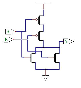
Exercise 110 Sketch a stick diagram for a CMOS 4-input NOR gate from Exercise 15.

. In this video stick diagram of CMOS EX-OR gate. Sketch a transistor-level schematic for a CMOS 4-input NOR gate. Draw the stick diagram for 21 MUX.
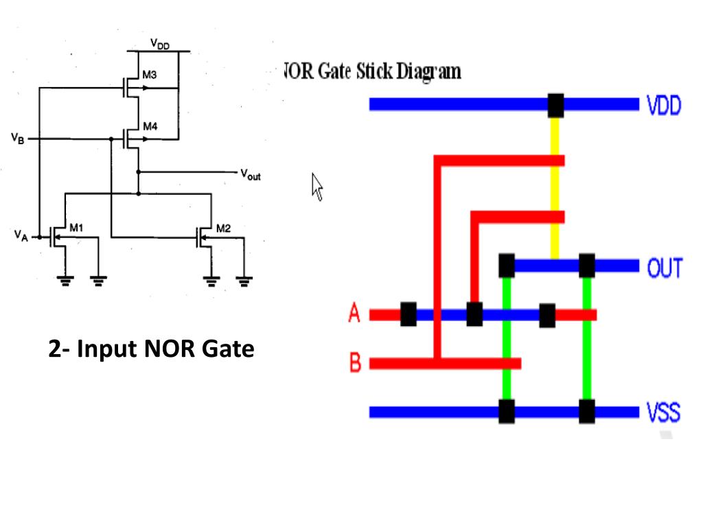
Interconnect Complementary transistor pairs share common. 2 Input NOR Gate TRUTH TABLE. Exercise 15 Sketch a transistor-level schematic for a CMOS 4-input NOR gate.
To understand the capabilities and limitations of stick diagram. Draw the stick diagram for two input NAND gate. An asynchronous sequential circuit is described by the following excitation andoutputfunctions 16Y x1x2 x1 x2 yZ y i Draw the logic diagram of the circuit.
In this video i have explained Stick Diagram of CMOS NOR Gate with following timecodes. Draw the stick diagram for two input CMOS NAND. Sketch a stick diagram for a cmos 4-input nor gate Senin 24 Oktober 2022 Now lets understand how this circuit will behave like a NAND gate.
Electrical Engineering questions and answers. Order gate wires on poly Step 2. EulerPaths CMOS VLSI Design Slide 4 4-Input NAND Gate Sticks Layout I1 I2 I3 I4 OUT Step 1.
We store cookies data. To learn how to draw stick diagrams for a given MOS circuit. Estimate the area from.
In all the 4 cases we have observed that V out is following the exact pattern as in the truth table for the corresponding input combination. To know what is meant by stick diagram. Sketch a stick diagram for a CMOS 4-input NOR gate.
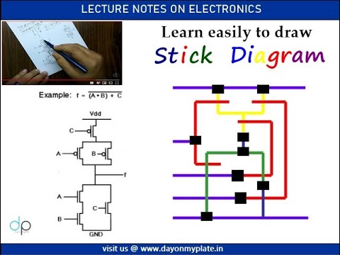
Tutorial On Stick Diagram To Design Cmos Vlsi Gates Day On My Plate Youtube
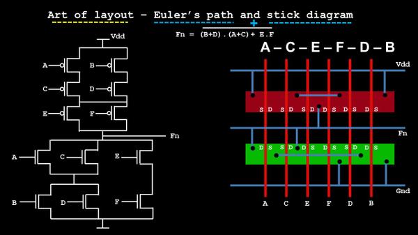
Art Of Layout Euler S Path And Stick Diagram Part 3 Vlsi System Design
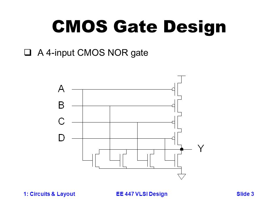
Vlsi Design Circuits Layout Ppt Video Online Download

Assignment 01 Pdf Assignment 01 1 Sketch A Transistor Level Schematic For A Cmos 4 Input Or Gate 2 Sketch A Transistor Level Schematic For A Course Hero
Solved 1 15 Sketch A Transistor Level Schematic For A Chegg Com
Ppt Purpose Of Design Rules Design Rules Interface Between Designer And Process Engineer Powerpoint Presentation Id 5803434
Layout Of Logic Gates Digital Cmos Design Electronics Tutorial
Combinational Mos Logic Circuits

Stick Diagram Of Two Input Cmos Nand Gate Compact Stick Diagram Explore The Way Youtube

Design Of Vlsi Systems Chapter 3

Solved Sketch A Transistor Level Schematic For A Cmos Chegg Com
How To Draw A Cmos Logic Diagram And Stick Diagram For A B Cd E A Quora

Norhayati Soin 05 Keee 4425 Week 7 1 23 8 2005 Lecture 9 Keee 4425 Week 7 Cmos Layout And Stick Diagram Cont D Ppt Download
Solved Problem 7 A Stick Diagram Has Been Put Together For A Chegg Com

Figure 4 14 From 4 Combinational Cmos Logic Circuits Cmos Logic Circuits Cmos Nor2 Two Input Nor Gate Semantic Scholar
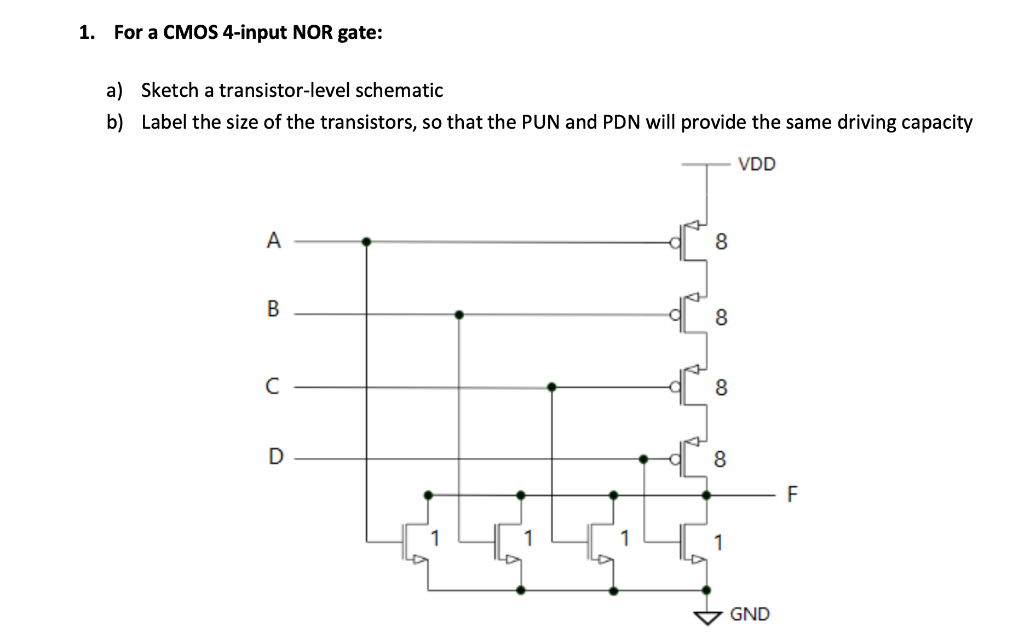
Solved 1 For A Cmos 4 Input Nor Gate A Sketch A Chegg Com
How To Draw A Cmos Logic Diagram And Stick Diagram For A B Cd E A Quora